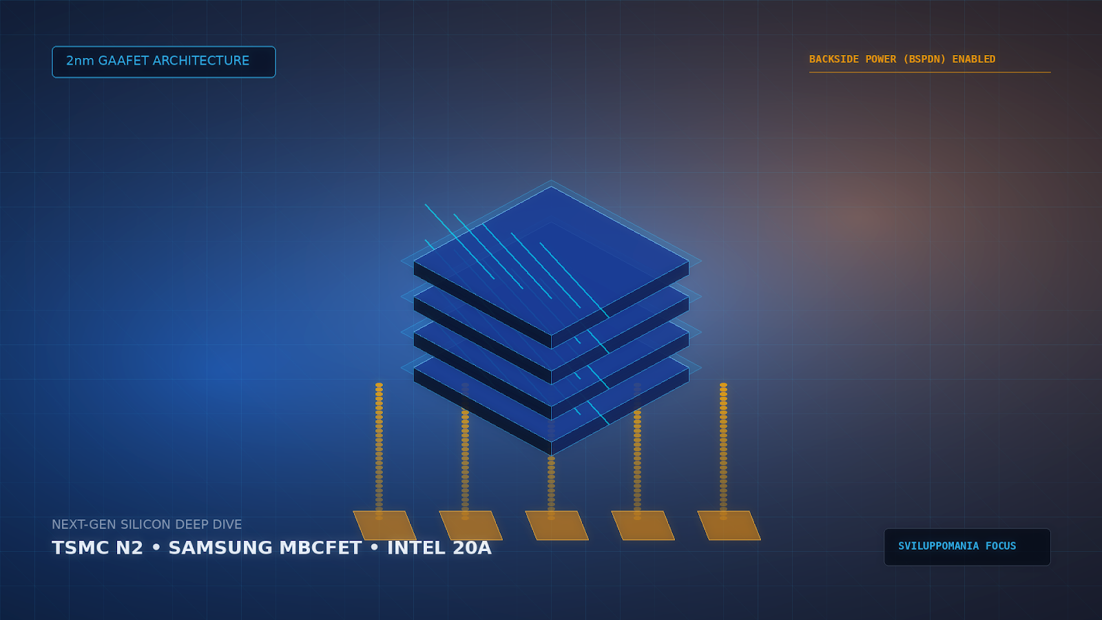
For more than half a century, Moore’s Law dictated the cadence of the tech industry by continuously driving logic gate scaling across flat surfaces. Over recent manufacturing cadences, however, classic geometric shrinkage collided with the fundamental limits of thermodynamics and quantum mechanics. The introduction of 2-nanometer (nm) class manufacturing nodes marks the most defining technological milestone in semiconductor physics over the last decade: phasing out three-dimensional FinFET topologies to implement stacked Gate-All-Around (GAAFET) nanosheets, paired with Backside Power Delivery Networks (BSPDN). This transition is far from a regular foundry shrink; it is a foundational re-architecting of how electrons navigate modern semiconductor channels.
Physical Constraints of Silicon and the Collapse of FinFET
Commercially deployed in the early 2010s to combat catastrophic parasitic leakage inherent to planar 2D transistors, FinFET (Fin Field-Effect Transistor) enabled the industry to scale reliably from 22nm down to dense 3nm processes. By elevating the conductive silicon channel as a three-dimensional vertical fin, the electrostatic gate managed to envelope the conduction path on three distinct boundaries (top, left, and right), applying sufficient electric field control to halt electron migration in the off-state.
Nevertheless, once physical gate lengths contracted below 12 nanometers and fin thicknesses reached atomic thresholds, the physics of semiconductor transport deteriorated. The critical barriers that halted further FinFET evolution below 3nm include:
- Sub-surface Quantum Tunneling: At tiny gate boundaries, charge carriers traverse the potential barrier via quantum tunneling, generating severe off-state parasitic leakage that inflates idle power draw and package thermals.
- Severe Drain-Induced Barrier Lowering (DIBL): Extreme proximity between source and drain regions lowers the electrostatic barrier height, degrading the gate’s ability to fully shut off the channel.
- Random Dopant Fluctuation (RDF): In atomic-scale channel volumes, minuscule deviations in dopant atom counts trigger significant threshold voltage (Vth) variations across adjacent dies.
The Mechanics of GAAFET: Horizontally Stacked Nanosheets
The definitive solution developed by materials scientists is the GAAFET (Gate-All-Around Field-Effect Transistor). While commercial foundries use varied marketing terminologies (TSMC retains GAA, Samsung brands it MBCFET – Multi-Bridge Channel FET, and Intel designates it as RibbonFET), the underlying physical principles remain identical.
In a GAAFET design, the vertical fin is turned horizontally and sliced into a vertical stack of ultra-thin, suspended silicon nanosheets. The high-k metal gate dielectric is chemically deposited so that it completely wraps around each individual nanosheet across all four sides in a 360-degree fashion.
This full structural confinement establishes complete electrostatic control: the gate exerts uniform electric force across the entirety of the channel cross-section, eliminating un-gated substrate leakage paths. Furthermore, unlike FinFET where fin height was locked to rigid etching depths, GAAFET nanosheet widths can be dynamically altered within standard cells (ranging from 15nm to over 50nm). Wider nanosheets deliver superior drive currents for maximum clock frequencies, while narrow nanosheets prioritize leak-free operation in idle logic blocks.
Backside Power Delivery Networks (BSPDN): Decoupling Power and Logic
Concurrent with channel redesigns, the implementation of Backside Power Delivery Networks (BSPDN)—known as Intel PowerVia or TSMC Super Power Rail (SPR)—represents an equally critical engineering achievement.
In conventional frontside manufacturing, both data signal routing and power distribution traces (Vdd and Vss) compete for metal interconnect layers above the active silicon channel. As logic density scaled, interconnect wires became microscopic, drastically elevating electrical resistance and generating significant voltage degradation, commonly known as IR Drop. A sizable percentage of total system power was wasted as parasitic thermal losses before reaching the active gates.
BSPDN completely overturns this design. The power delivery network is migrated entirely to the rear side of the processed silicon wafer. The silicon substrate is polished and thinned to a thickness of mere micrometers, allowing high-gauge backside power rails to supply the active cells directly using vertical Nano-Through Silicon Vias (Nano-TSVs). Key operational advantages include:
- Elimination of IR Voltage Drops: Power delivery resistance decreases by 15% to 30%, enabling logic clusters to operate reliably at reduced minimum supply voltages (Vmin).
- Decongested Signal Interconnects: The frontside metal stack is reserved strictly for high-speed signal routing, minimizing parasitic wire-to-wire capacitance and driving higher clocks under strict thermal envelopes.
- Standard Cell Area Optimization: Standard logic cells contract by an additional 10% to 15% in layout footprint without requiring expensive double-patterning EUV iterations.
Comparative Architecture Matrix: Metric Breakdown
The quantifiable improvements transitioning from mature 3nm-class FinFET manufacturing to 2nm-class GAAFET with Backside Power Delivery are detailed below:
| Architectural Metric | 3nm Process (Optimized FinFET) | 2nm Process (GAAFET + BSPDN) | Engineering Impact |
|---|---|---|---|
| Gate Confinement | Tri-Gate (Enclosing 3 fin sides) | Gate-All-Around (360° Wrapped Nanosheets) | Near-total elimination of subthreshold leakage |
| Logic Density (MTr/mm²) | ~220 – 280 MTr/mm² | ~340 – 400 MTr/mm² | Roughly +20% effective logic density expansion |
| Minimum Supply Voltage (Vmin) | ~0.65V – 0.70V | ~0.52V – 0.58V | Stable ultra-low voltage performance scaling |
| Power Routing Plane | Frontside Layer (Shared logic/power stacks) | Backside Layer (Wafer rear-side direct) | Substantial IR drop suppression & thermal headroom |
| Iso-Frequency Efficiency | Baseline Target | -25% to -30% power consumption | Sustained high compute execution envelopes |
Practical Real-World Impact: Edge NPUs to Hyperscale Infrastructure
How does this transition alter actual computing experiences? In mobile hardware, mitigating idle thermal dissipation solves one of modern computing’s toughest bottlenecks: persistent on-device artificial intelligence execution.
Large multimodal generative models and computer vision matrices require massive, sustained activation of Neural Processing Units (NPUs). In 3nm FinFET chips, thermal hotspots quickly build up inside tiny core areas, triggering aggressive kernel throttling to prevent chassis overheating. With 2nm GAAFET electrostatic control and BSPDN power routing, modern mobile chips can sustain on-device neural inferencing workloads under strict 3-to-4-Watt power budgets without thermal throttling.
Meanwhile, in cloud infrastructure and enterprise training clusters, a 20% drop in overall power loss scales exponentially. Slashing server farm Power Usage Effectiveness (PUE) metrics and enabling higher sustained multi-chiplet clock frequencies directly yields millions of kilowatt-hours in operational savings.
Frequently Asked Questions (FAQ)
Does 2nm simply mean longer smartphone battery life?
Not necessarily. Architectural gains are rarely reserved solely for idle power savings. Chip designers convert the widened thermal headroom into higher compute capabilities: expanding Neural Processing Unit TOPS throughput, fitting larger on-die cache hierarchies, and sustaining continuous peak graphics performance without thermal degradation.
What is the primary difference between RibbonFET, MBCFET, and GAAFET?
These terms represent proprietary implementations of the same fundamental physics: Gate-All-Around technology. GAAFET is the industry-standard engineering term; MBCFET (Multi-Bridge Channel FET) is Samsung’s trademarked nomenclature; RibbonFET is Intel’s proprietary brand for its nanosheet architecture.
Why is Backside Power Delivery (BSPDN) so challenging to manufacture?
BSPDN requires processing both surfaces of a wafer. After fabricating standard frontside transistors, the wafer must be bonded to a carrier handle, flipped, mechanically thinned down to micro-scale levels, and etched with atomic accuracy to align vertical Nano-TSVs with standard cells, demanding alignment tolerances of under a few nanometers.
When will 2nm devices reach mainstream consumers?
High-volume commercial output initiated across 2026 pipelines. Adoption adheres to typical industry rollout patterns: starting in ultra-premium mobile SoCs and enterprise hyperscale accelerators, followed by mainstream desktop platforms and consumer components in the quarters ahead.
Enjoyed This Deep Dive?
Stay ahead of the curve with real-time tech news and analyses. Get the official SviluppoMania app on your device.
 |
|
|